This 12V uninterruptible power supply initially designs to drive my fiber optic modem/router. The key reason to build this power supply is to get continuous internet and phone connection during power failures. Core components of this power supply are a constant voltage charger, 12V DC power supply, AC line monitoring unit, and 12V high capacity sealed lead-acid battery. The entire system designs using locally available components.
 |
| Prototype version of 12V UPS system |
The charging circuit of this system builds around using the popular LM350 voltage regulator. This regulator calibrates to provide both 14.4V fast charging and 13.6V trickle charging. Based on the condition of the battery, the MCU will determine the appropriate charging mode.
At the online state, the LM2576-12 switching regulator provides 12V output to the driving system. (in my arrangement, a fiber optic router).
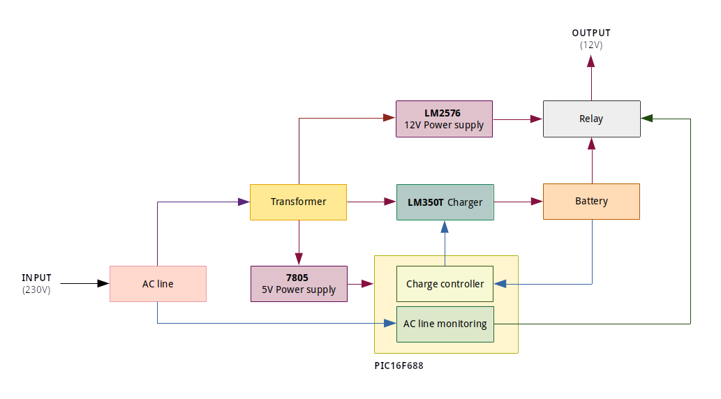 |
| Block diagram of the 12V UPS system |
The PIC16F688 MCU monitors the AC line and battery to controls the output voltage of the LM350 regulator and the output relay. The firmware of this MCU written using the Microchip XC8 compiler, and all the source code and configuration files are available to download at the project repository at GitHub.
The sealed 12V lead-acid battery is the most crucial component of this unit. 12V, 9Ah battery is the most recommended for this system. At the time of this writing, this battery cost around Rs. 3500 (US$ 17.60), and I bought it from a local online store.
In online mode, this system provides 12V output. In offline mode, if it has a fully charged battery, it delivers an output of 12.5V.
This uninterruptible power supply is suitable for appliances that need 12V - 13V input with a maximum of 2A current. With the configuration described above, this system continued to power my Huawei HG8245H5 fiber optic router for more than 7 hours.
This power supply unit is an open hardware project. All the schematic, PCB design files, firmware source codes, and compiled binaries are available to download at the project repository at GitHub.
Assembling the circuit
In the provided design, all the parts used in the PCB are through-hole-type components. For this design, we used low-cost and commonly available electronic components.
The recommended transformer for this system is the 230V to 15V×2 (5A) and 12V×2 (500mA) step-down transformer.
Install adequate heatsinks for LM350, LM2576, and 7805 regulators. To minimize the space, we recommend using a single heatsink for LM350 and LM2576 regulators. If using a single heatsink, always be sure to install ceramic and mica insulators to the LM2576 regulator to eliminate short circuits.
The PCB provided with this project is design to be constructed using a single-sided copper board. The dimensions of the PCB are 131.7mm × 100mm.
Use 1% ¼W metal film resistors for R3, R7, and R8 to get accurate results. For R2 and R4, use 3W or higher rated ceramic cement resistors.
Calibration and testing
Before connecting the load and battery to the system, it is necessary to follow the below steps to calibrate the system.
- Remove PIC16F688 MCU from the U2 socket.
- Short circuit pin 1 and 7 of the U2 socket.
- Connect digital multimeter to the cathode of the D3 diode.
- Set RV2 until the multimeter indicates 13.6V.
- Connect pin 7 and 14 of the U2 socket.
- Now adjust RV3 until the multimeter indicates 14.4V.
- Connect PIC16F688 MCU to the U2 socket.
After finishing the above steps, connect the 5V UART-to-USB adapter to the J6 debug terminal and initiate the serial terminal with a baud rate of 1200 with an 8N1 configuration.
 |
| Test setup of the 12V UPS system |
Connect the digital multimeter to battery terminals and adjust RV1 until the serial terminal shows the ten times voltage reading of the digital multimeter. (Example: 12.6V is displaying on the serial terminal as 126)
After the above calibration, the system is now ready to use. Initially connect the battery to the system, and leave it until it got fully charged.
This PCB directly connected to the AC mains, and always be sure to use the necessary precautions when reading voltages and at the calibration.
Comments
I was looking for this