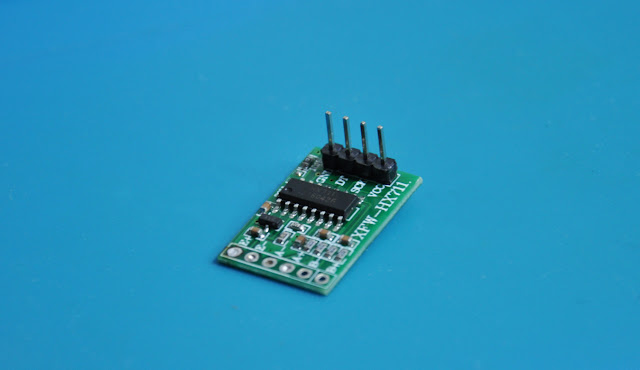
The HX711 is a versatile integrated circuit (IC) designed for precision analog-to-digital (A/D) conversion, particularly suited for strain gauge load cell applications. It features a 24-bit A/D converter with a differential input stage capable of handling both single-ended and differential input signals. Additionally, this device offers adjustable gain amplification to accommodate various load cell sensitivities.
 |
| HX711 module. |
A common module based on the HX711 available in the market, including on AliExpress, is shown below. This module utilizes its internal analog supply regulator, which ensures a stable analog supply (AVDD) for the ADC and other internal components. The output voltage of the regulator (AVDD) is calculated using the following formula: VAVDD = VBG × (R1 + R2) / R2.
 |
| AVDD voltage test setup. |
According to the electrical characteristics listed in the datasheet, the reference bypass voltage (VBG) is 1.25V. For the modules mentioned, R1 is set at 8.2kΩ and R2 at 20kΩ. By substituting these values into the formula, we calculate AVDD to be approximately 4.29V.
 |
| Actual AVDD voltage on unmodified HX711 module. |
The HX711 IC operates within a voltage range of 2.6V to 5.5V. However, many HX711 modules on the market come with an internal voltage regulator that outputs approximately 4.29V. This can pose challenges when using the module with 3.3V microcontrollers. Furthermore, the datasheet specifies that the output voltage of the regulator should be at least 100mV lower than the supply voltage (VSUP), making the current regulator's output voltage incompatible with 3.3V supply voltages.
 |
| R1 and R2 resistors in HX711 module. |
To address this, we need to ensure that AVDD is within the 2.6V to 3.2V range to make the module compatible with both 3.3V and 5V systems. After conducting some calculations, we determined that replacing R1 with 10kΩ and R2 with either 15kΩ or 12kΩ would be ideal. Using a 15kΩ resistor gives an AVDD of 3.1V, while using a 12kΩ resistor reduces it to 2.75V. In one of our experimental boards, we opted to replace R2 with a 12kΩ resistor.
 |
| Interchanged R1 and R2. |
As a further test, we lowered the AVDD to approximately 1.6V, and at this voltage, the HX711 still produced the correct results in our test setup. Interestingly, we observed that swapping R1 and R2 allows us to achieve an AVDD of 1.76V. To test this, we swapped R1 (8.2kΩ) and R2 (20kΩ) in one of the modules, and after applying a 5V supply, we noted that the AVDD returned at 1.65V, with the HX711 still providing correct outputs.
 |
| AVDD reading after interchanging R1 and R2. |
To evaluate the boards, we created a quick prototype using the STM32F405 MCU. In this prototype, we powered the HX711 module with 3.3V and directly connected its I/O pins to the STM32 GPIO pins.
For interaction with the module, we utilized the HX711 library provided at https://github.com/PCov3r/HX711-STM32-Library. The source code for our test firmware is available here.
 |
| Sample readings from the HX711 with 20kg load-cell. |
After making the above modifications, all modules produce a stable output at 3.3V. We tested these modules with both 3.3V and 5V MCUs, using 5kg, 10kg, and 20kg load cells, and it operated correctly across all these combinations.
Comments